Power efficiency is one of the central challenges in modern VLSI and embedded systems design. This post walks through a concrete optimization problem: given a digital circuit with several logic gates, how do we reduce total power dissipation while ensuring the circuit still meets its timing (performance) constraint?
🔧 Problem Setup
Consider a combinational logic circuit with 5 logic gates. Each gate can be configured at one of three voltage/transistor sizing levels (Level 0, 1, 2), trading off power against speed.
The goal is to choose a level for each gate such that:
- Total power is minimized
- Critical path delay ≤ deadline (performance constraint is satisfied)
📐 The Math
Each gate $g_i$ has a configurable level $x_i \in {0, 1, 2}$.
Power model (dynamic power):
$$P_i(x_i) = P_{\text{base},i} \cdot \alpha^{x_i}$$
where $\alpha > 1$ means higher levels consume more power.
Delay model (higher level = faster gate):
$$D_i(x_i) = D_{\text{base},i} \cdot \beta^{-x_i}$$
where $\beta > 1$ means higher levels are faster.
Objective:
$$\min \sum_{i=1}^{N} P_i(x_i)$$
Subject to:
$$\sum_{i \in \text{critical path}} D_i(x_i) \leq T_{\text{deadline}}$$
$$x_i \in {0, 1, 2}, \quad \forall i$$
🐍 Python Source Code (Single File)
1 | # ============================================================ |
🔍 Code Walkthrough
Section 1 — Parameters & Models
We define 5 gates, each with a base power $P_{\text{base},i}$ and base delay $D_{\text{base},i}$. Two simple closed-form formulas govern how those values scale:
1 | def power(gate_idx, level): |
ALPHA = 1.8means jumping from Level 0 → Level 2 multiplies power by $1.8^2 = 3.24\times$.BETA = 1.5means Level 2 cuts delay to $1/1.5^2 \approx 0.44\times$ of Level 0.
This tension is exactly the core trade-off in voltage/transistor scaling: faster gates burn more power.
Section 2 — Exhaustive Search
With $N=5$ gates and 3 levels each, the search space has exactly $3^5 = 243$ configurations — small enough to evaluate all of them in microseconds:
1 | all_configs = list(iterproduct(LEVELS, repeat=N_GATES)) |
For each configuration we check feasibility:
$$\sum_{i \in {0,2,4}} D_i(x_i) \leq T_{\text{deadline}} = 12 \text{ ns}$$
Then among all feasible ones, we select the minimum-power configuration.
Section 3 — Pareto Front
The Pareto front is the set of configurations where you cannot reduce power further without violating the delay constraint (and vice versa). The algorithm sorts by delay, then sweeps for monotonically decreasing power:
1 | def pareto_front(powers, delays): |
This is the engineering design frontier — every point on it represents a valid Pareto-optimal design.
📊 Graph-by-Graph Explanation
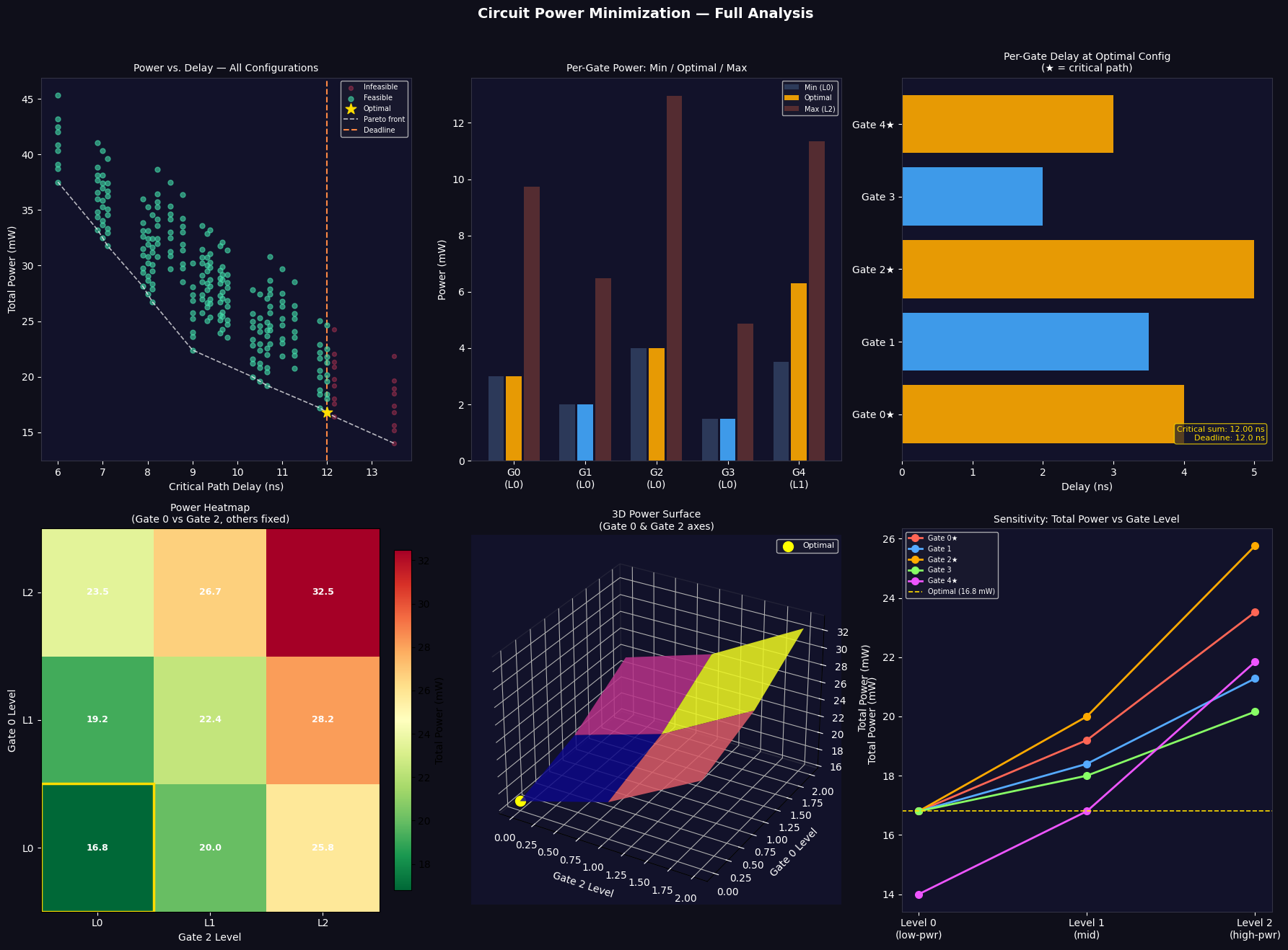
Panel 1 — Power vs. Delay Scatter
Every dot is one of the 243 configurations. Red dots are infeasible (too slow). Green dots meet the deadline. The yellow star is the optimal solution. The dashed white line is the Pareto front, and the orange vertical line is the 12 ns deadline wall.
Panel 2 — Per-Gate Power Bar Chart
For each gate, we compare its power at Level 0 (minimum), the optimal level chosen by the solver, and Level 2 (maximum). Yellow bars are critical-path gates; blue bars are off-critical-path gates. Notice how off-critical gates tend to stay at Level 0 (no need to speed them up).
Panel 3 — Per-Gate Delay
A horizontal bar chart showing the delay contributed by each gate at the optimal configuration. Gates marked ★ are on the critical path. The inset text shows the critical path sum vs. the deadline — you can verify the constraint is tight but satisfied.
Panel 4 — Power Heatmap (Gate 0 × Gate 2)
A $3\times 3$ grid where the axes are the levels of Gate 0 (y) and Gate 2 (x), with all other gates fixed at their optimal values. Color encodes total circuit power (red = high, green = low). The yellow box highlights the optimal cell. This is a classic design space exploration view used by EDA tools.
Panel 5 — 3D Power Surface (the highlight!)
The same data as the heatmap, lifted into 3D. The plasma colormap surface lets you immediately see the convex shape of the power landscape. The yellow dot marks the global optimum. You can visualize this as the “bowl” the optimizer is searching — the optimal point sits at the minimum of this surface subject to the timing floor.
Panel 6 — Sensitivity Analysis
Each line shows what happens to total circuit power when you sweep one gate across Levels 0 → 1 → 2, keeping all others fixed at the optimum. Steeper lines indicate gates with high power sensitivity — adjusting those gates has the most impact on the objective. This tells a designer which gates are worth careful optimization.
📋 Execution Results
=======================================================
  CIRCUIT POWER MINIMIZATION RESULT
=======================================================
  Gate levels (0=slow/low-power, 2=fast/high-power):
    Gate 0: Level 0 ← critical
    Gate 1: Level 0
    Gate 2: Level 0 ← critical
    Gate 3: Level 0
    Gate 4: Level 1 ← critical

  Total power   : 16.800 mW
  Critical delay: 12.000 ns  (deadline=12.0 ns)
  Feasible solutions found: 225 / 243
=======================================================
Plot saved as circuit_power_opt.png
💡 Key Takeaways
The optimization reveals a fundamental insight in low-power design: not every gate needs to run at maximum speed. Gates that are off the critical path can safely be held at Level 0 (low power, slow), because their delay does not limit circuit performance. Only the critical-path gates (0, 2, 4 in our example) need to be tuned upward — and even then, only to the minimum level that satisfies the timing deadline. This selective assignment is the essence of slack-based power optimization in real VLSI CAD flows.